Is the single-cycle design realistic?
Lecture 4 – Register Transfer & Datapath Design, Control Unit Design, and Instruction Set Architecture (ISA)
Build the CPU from the ground up: ISA choices, RTL register transfers, single-cycle datapath, and hardwired vs microprogrammed control with examples.
ISA vs Microarchitecture (what vs how)
- ISA (what): programmer-visible instructions, registers, addressing modes, exceptions, and the binary encoding (opcode + fields).
- Microarchitecture (how): the implementation datapath, control, pipeline depth, cache sizes, TLB, etc. Multiple µ-architectures can implement the same ISA.
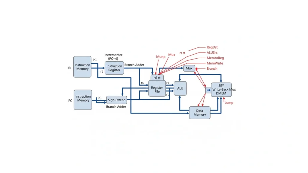
Register Transfer Level (RTL) Basics
Registers: PC, general-purpose register file (e.g., 32 × 32-bit), IR (optional).
ALU: add/sub/and/or/slt, plus zero flag.
Memories: Instruction Memory (IMEM), Data Memory (DMEM).
Muxes & Extenders: ImmExt (sign/zero extend), sources to ALU and write-back paths.
Example RTL for a typical instruction cycle (single-cycle view):
- IF:
IR ← IMEM[PC]; PC ← PC + 4 - ID:
A ← RF[rs]; B ← RF[rt]; ImmExt ← SignExt(imm) - EX (R-type ADD):
ALUout ← A + B - EX (I-type LW/SW):
ALUout ← A + ImmExt - MEM (LW):
MDR ← DMEM[ALUout] - WB (LW):
RF[rt] ← MDR; WB (ADD):RF[rd] ← ALUout
A Compact Single-Cycle Datapath (RISC-style)
Instruction formats:
- R-type:
op(6) rs(5) rt(5) rd(5) shamt(5) funct(6) - I-type:
op(6) rs(5) rt(5) imm(16) - J-type:
op(6) target(26)
Control signals (classic set):
RegDst, ALUSrc, MemtoReg, RegWrite, MemRead, MemWrite, Branch, Jump, ALUOp[1:0]
Encoding sketch (typical):
- ADD (R):
RegDst=1, ALUSrc=0, MemtoReg=0, RegWrite=1, MemRead=0, MemWrite=0, Branch=0, Jump=0, ALUOp=10 - SUB (R): same as ADD but ALUOp selects SUB via
funct. - LW (I):
RegDst=0, ALUSrc=1, MemtoReg=1, RegWrite=1, MemRead=1, MemWrite=0, Branch=0, Jump=0, ALUOp=00 - SW (I):
ALUSrc=1, RegWrite=0, MemRead=0, MemWrite=1(others 0),ALUOp=00 - BEQ (I):
ALUSrc=0, RegWrite=0, Branch=1, ALUOp=01(ALU does A−B; if zero → branch) - J (J):
Jump=1
Branch target:
PC ← PC+4 + (SignExt(imm) << 2)whenZero=1andBranch=1.
Jump target:PC ← {PC+4[31:28], target, 2’b00}whenJump=1.
Control Unit Design
Hardwired (combinational + small decoder)
- Main Decoder: opcode → the 8 control bits above.
- ALU Decoder:
(ALUOp, funct) → ALUControl(ADD, SUB, AND, OR, SLT…). - Pros: fast and simple for small ISAs. Cons: hard to extend (e.g., many addressing modes).
Truth-table snippet (illustrative):
| Opcode | RegDst | ALUSrc | MemtoReg | RegWrite | MemRead | MemWrite | Branch | Jump | ALUOp |
|---|---|---|---|---|---|---|---|---|---|
| R-type | 1 | 0 | 0 | 1 | 0 | 0 | 0 | 0 | 10 |
| LW | 0 | 1 | 1 | 1 | 1 | 0 | 0 | 0 | 00 |
| SW | X | 1 | X | 0 | 0 | 1 | 0 | 0 | 00 |
| BEQ | X | 0 | X | 0 | 0 | 0 | 1 | 0 | 01 |
| J | X | X | X | 0 | 0 | 0 | 0 | 1 | XX |
(X = don’t care)
Lecture 3: Cache Memory Deep Dive Locality, Mapping, Write Policies, TLB & Prefetching

Microprogrammed (control store)
- Each instruction executes as a sequence of micro-instructions stored in a control memory.
- Micro-instruction fields set datapath control lines (e.g.,
SRC_A,SRC_B,ALU_FUN,REG_WE,MEM_RD,PC_SRC,COND,NEXT). - Pros: easier to add complex instructions; patchable. Cons: typically slower than hardwired.
Tiny micro-sequence (example for LW):
IF: IR←IMEM[PC]; PC←PC+4EX: ALUout←RF[rs]+SignExt(imm)MEM: MDR←DMEM[ALUout]WB: RF[rt]←MDR
Worked Example (R-type ADD)
Instruction: add $t0,$t1,$t2
- ID:
A←RF[$t1],B←RF[$t2] - EX:
ALUout←A+B(ALUControl=ADD) - WB:
RF[$t0]←ALUout
Control:RegDst=1, ALUSrc=0, MemtoReg=0, RegWrite=1, ALUOp=10.
RTL/Verilog Mini-ALU
// 32-bit ALU (ADD, SUB, AND, OR, SLT)
module alu(input [31:0] A, B,
           input [2:0] op,        // 000=ADD,001=SUB,010=AND,011=OR,100=SLT
           output reg [31:0] Y,
           output zero);
  always @(*) begin
    case(op)
      3'b000: Y = A + B;
      3'b001: Y = A - B;
      3'b010: Y = A & B;
      3'b011: Y = A | B;
      3'b100: Y = ($signed(A) < $signed(B)) ? 32'd1 : 32'd0;
      default: Y = 32'd0;
    endcase
  end
  assign zero = (Y == 32'd0);
endmodule
Mini-Lab
- Paper design: Draw the single-cycle datapath with labeled buses and the 8 control signals.
- Control table: Fill the table rows for
ADD, SUB, LW, SW, BEQ, J. - (Tool) In Logisim-evolution (or your preferred simulator):
- Build a 32-bit ALU and a small register file (2 read, 1 write port).
- Show a working
LWfollowed byADDandSWusing hand-loaded IMEM/DMEM contents.
- Question: Where would a sign-extend block sit? Why not zero-extend for
LWaddress arithmetic?
Quick Check (with answers)
- What does RegDst control? → Whether destination register is
rd(R-type) orrt(I-type). - How is BEQ implemented in the datapath? → ALU does
A−B, test Zero, and selectPC+4+(imm<<2)ifBranch=1. - Why prefer hardwired control for a tiny RISC? → Faster and simpler.
- When might you choose microcode? → Complex ISAs or when you need patchable control.
- Which signals must be 1 for LW in a single cycle? →
ALUSrc, MemtoReg, RegWrite, MemRead.
The approach followed at E Lectures reflects both academic depth and easy-to-understand explanations.
People also ask:
It’s great for teaching but slow at scale; real CPUs pipeline stages for higher clock rates.
Either in a dedicated shifter or by wiring the low bits to 00 and adding to PC+4.
Yes, but many diagrams show a separate adder for clarity (timing/structure reasons).
With the classic 8 signals + ALUControl, you can implement a rich MIPS-like subset.
Have students write small MIPS-style programs (LW, ADD, SW, BEQ) and trace the control lines per instruction.