
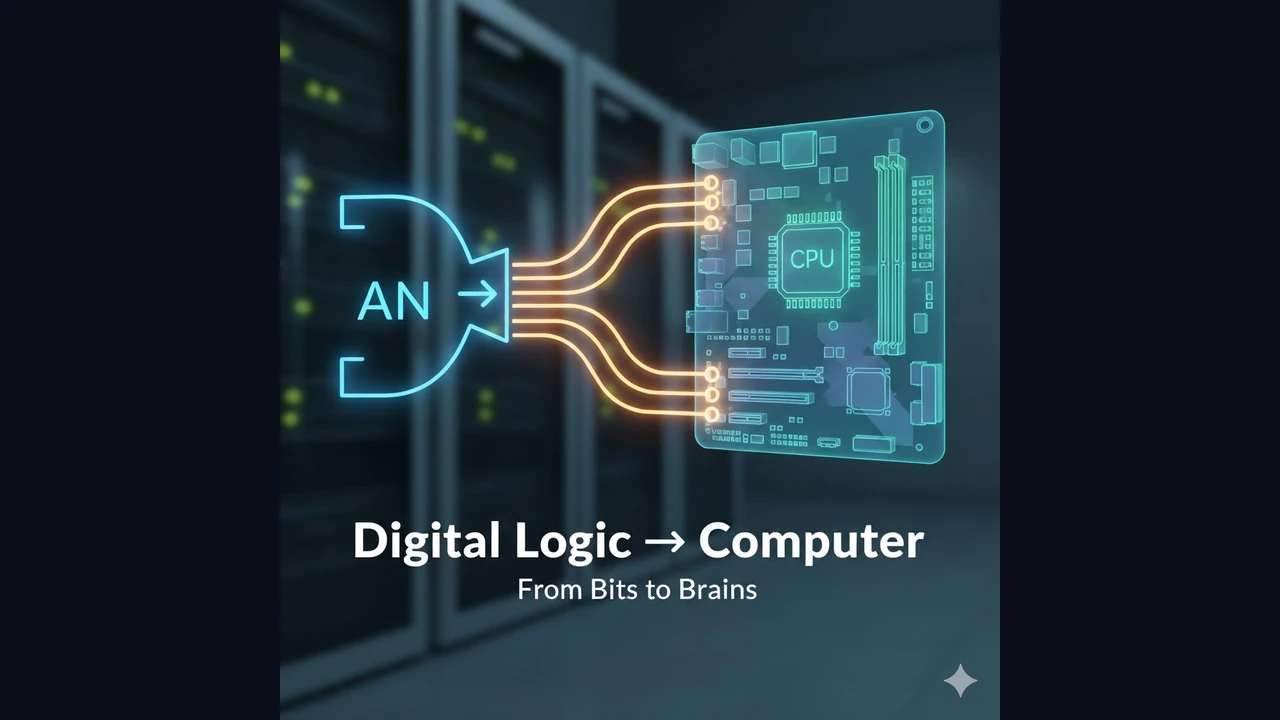
Digital logic design from bits to CPU numbers, gates, K-maps, combinational & sequential circuits and how programs run on CPU, memory, and I/O.
Number Systems (Decimal, Binary, Hex)
- Binary ↔ Decimal:
1011₂ = 8+2+1 = 11₁₀. - Binary ↔ Hex: group bits in 4s:
1101 1010₂ = DA₁₆. - Signed integers: Two’s complement encodes negatives by inverting bits and adding 1 (single zero, easy arithmetic).
Quick task: Convert 29₁₀ to binary and hex → 11101₂, 1D₁₆.
Boolean Algebra Essentials
Operators: NOT (¬A), AND (A·B), OR (A+B), XOR (A ⊕ B).
Core laws: Commutative, Associative, Distributive, Identity, Complement, De Morgan.
Example simplificationF = A·B + A·B‘ → factor A: F = A(B + B') = A.
Logic Gates & Truth Tables
| Gate | Symbolic form | When output is 1 |
|---|---|---|
| NOT | A’ | when A=0 |
| AND | A·B | both inputs 1 |
| OR | A+B | any input 1 |
| XOR | A ⊕ B | inputs differ |
| NAND | (A·B)’ | unless both 1 |
| NOR | (A+B)’ | only when all 0 |
Tip: NAND/NOR are universal any circuit can be built from them.
Combinational Logic (No Memory)
Output depends only on current inputs.
Typical blocks:
- Adders (half/full adder, ripple carry), comparators
- Multiplexers (select input by control), decoders/encoders
- ALU slices inside CPUs
Hands-on: Design a 4-to-1 MUX using basic gates; verify with a truth table.
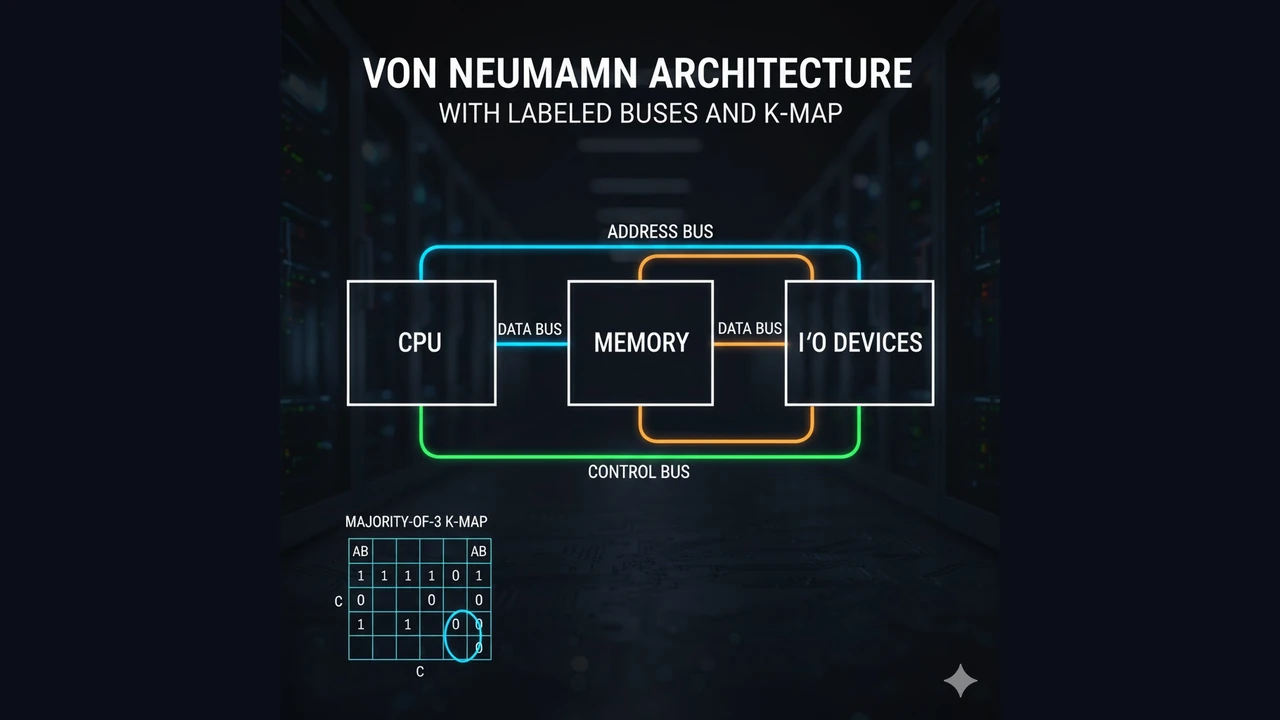
Karnaugh Maps (K-maps) for Minimization
Visual method to reduce sum-of-products.
Example: Majority-of-3 F(A,B,C)=1 when at least two inputs are 1.
Grouping 1s on a 3-variable K-map yields:F = A·B + A·C + B·C (three 2-input ANDs into one OR).
Sequential Logic (With Memory)
Output depends on inputs + stored state.
Latches & Flip-Flops
- SR latch, D latch (level-sensitive)
- D flip-flop (edge-triggered): captures input on clock edge → used to build registers.
Registers & Counters
- Register: N flip-flops storing N bits.
- Counter: register + next-state logic (up/down, modulo-N).
- FSMs: finite-state machines with state register + next state/output logic (Mealy/Moore).
Hands-on: Draw a 2-bit synchronous counter (00→01→10→11→00). List the state table and implement with D flip-flops.
From Circuits to Computers: CPU Memory I/O
Most systems follow the von Neumann model:
- CPU = Control unit + ALU + Registers/Flags
- Memory stores instructions & data
- I/O devices interact with the outside world
- Buses (address, data, control) carry values and timing signals
Fetch Decode Execute (high level)
- Fetch instruction at PC from memory to IR.
- Decode opcode & addressing mode.
- Execute via ALU, register transfers, or memory I/O; update flags and PC.
Example: mapping C to hardware
y = a + b;- CPU loads
aandb(two memory reads over the bus). - ALU adds registers → sets flags (ZF, CF, OF…).
- CPU stores result to
y(memory write).
Hardware vs Software Layers
Applications → OS → Compiler/Assembler → ISA → Microarchitecture → Gates → Transistors.
Programs target the ISA; many microarchitectures (pipelines, caches, branch predictors) can implement the same ISA underneath.
Summary
Digital logic design turns bits into gates, gates into circuits, and circuits into the CPU that runs your code. With numbers, Boolean laws, K-maps, and the CPU–Memory–I/O model, you now have the foundation to study instruction formats, addressing modes, and performance next.
Key Terms
ALU, Register, Flag, Bus, IR (instruction register), PC (program counter), Two’s complement, K-map, Flip-flop, FSM, ISA, von Neumann.
The approach followed at E Lectures reflects both academic depth and easy-to-understand explanations.
People also ask:
It lets the same adder handle +/−, has a single zero, and simplifies overflow checks.
They visually group 1s (or 0s) to remove redundant literals, producing smaller, faster circuits.
Combinational depends only on current inputs; sequential also depends on stored state (flip-flops/registers).
It orchestrates fetch decode execute: generates control signals for the ALU, registers, memory, and I/O.
Yes any Boolean function can be implemented using only NANDs or only NORs.